サブサーキットとVerilog-Aを使ったアキシャル抵抗と表面実装抵抗の回路モデル
Mike Brinson
Copyright 2014, 2015 Mike Brinson, Centre for Communications Technology, London Metropolitan University, London, UK. (mailto:mbrin72043@yahoo.co.uk)
Permission is granted to copy, distribute and/or modify this document under the terms of the GNU Free Documentation License, Version 1.1 or any later version published by the Free Software Foundation.
はじめに
抵抗は、電子回路設計において基本的な構成要素の1つです。多くの場合、従来の抵抗の回路シミュレーションモデルは、オームの法則で指定されるI/V特性により特徴付けられます。現実には、RF抵抗のインピーダンスは周波数依存であり、部品の物理特性、部品の製造技術、それから部品が回路中でどのように接続されているかにより決まります。低周波では、固定抵抗は室温であるノミナル値をもちオームの法則で正確にモデルされます。RF周波数では、抵抗はインダクタンスやキャパシタンスのように振る舞うことが多いという事実が、回路が設計通り動くかどうかを決める決定的な役割を演じます。同様に、もしも抵抗が著しくリアクタンス性の特性を示す周波数において理想的な部品とモデル化されるなら、シミュレーション結果は恐らく不正確です。このQucsノートで紹介するサブサーキットとVerilog-Aのコンパクトな抵抗モデルは、低周波から数GHzを超えないRF周波数に渡り、良好な特性を与えるように設計されています。
RF抵抗モデル
Qucsの線形抵抗モデルの回路図シンボル、I/V方程式とパラメータを図1に示します。このモデルと対照的に、図2はプリント回路基板(PCB)にマウントされた金属膜(MF)のアキシャルRF抵抗(a)、そのQucsの回路図シンボル(b)と等価回路モデル(c)を図示します。薄膜表面実装(SMD)抵抗も図2(c)のモデルで表現することができます。
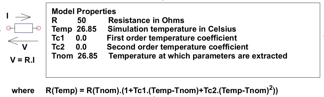 図1 - Qucsの組み込み抵抗モデル
アキシャルまたはSMDの抵抗の最大の寸法が、最小の信号波長の約20倍以下の信号周波数では、抵抗は、小さな直列インダクタンス Ls と Rs の抵抗とそれらと並列な寄生容量 Cp からなる集中定数の受動回路でモデル化できます。図2で、 Rs はパラメータを抽出した温度 Tnom での抵抗のノミナル値、 Ls は Rs に付随するインダクタンスを表し、 Ls の値は主に部品製造業者が Rs の値を指定された誤差範囲に収めるために採用するトリミング手法によって決まります。同様に、容量 Cp は、 Rs に関連する寄生容量をモデル化し、 Cp の値は Rs の物理寸法の関数です。RF周波数では、導線の寄生要素を図2の赤色で描いたボックスの中の内部の等価回路モデルに加えることが、正確な動作のために重要です。図2で Llead と Cshunt は、抵抗に直列な導線インダクタンスとグランドへの並列容量をそれぞれ示しています。
図2 - PCBにマウントした抵抗:(a)マウントしたアキシャル部品、(b)Qucsシンボル、(c)等価回路モデル
51Ωの金属膜(MF)アキシャル抵抗の典型的なモデルパラメータセットは(1) LS=8nH, Cp=1pF, Llead=1nH, Cshut=0.1pF です。図3に描かれているのは、RF抵抗のSパラメータを1MHzから1.3GHzの周波数範囲で測定する基本的なSパラメータ用テストベンチ回路です。この例はまたSパラメータのシミュレーションデータからいかに抵抗モデルおインピーダンスの実部と虚部を取り出すことができるかを説明しています。図3のグラフは、前述したような図2の等価回路に示した典型的な金属膜抵抗のインピーダンスが、1MHzから1.3GHzの高周波帯において周波数の強い関数であることを明確に示しています。
図3 - MFアキシャル抵抗のためのQucsのSパラメータシミュレーション用テスト回路とプロットした出力データ:Rs=51 , Ls=8nH, Cp=1pF, Llead=1nH, Cshunt=0.1pF
RF抵抗モデルの解析
部品レベルに対し提案されたRF抵抗モデルを図4に示す。


図4 - 図のテスト回路に合わせて90度回転し端子の1つを接地したRF抵抗モデル。モデルの各部はモデルのインピーダンスZの計算のためにグループ化して示す。
図5はモデルのシミュレーションとシミュレーションデータの後処理のために一連の理論式がどのようにQucsの式に変換できるかを説明しています。この例で、Qucsの式 Eqn1 はRF抵抗モデルのパラメータ値を持ち、Qucsの式 Eqn2 は、この節のはじめに導入されたモデル式のリストです。図5は、また1MHzから1.3GHzの周波数帯で、 ZXR と ZI とその他の計算項が周波数によりどのように変化するかを示す直交座標系のグラフを表示しています。
図5 - Qucsの後処理の仕組みを使ってRF抵抗のインピーダンスZを理論解析: Qucsの解析計算を終了させるために、ダミーのシミュレーションアイコン(この例ではDCシミュレーション)が必要なことに注意
インピーダンス測定器をシミュレーションしたRF抵抗インピーダンス直接測定の方法
図6に、単純なインピーダンス測定器
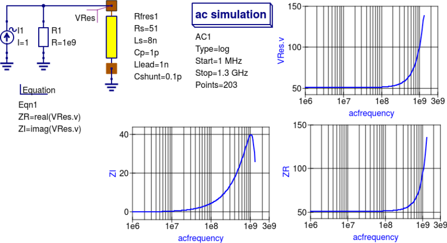 Figure 6 -A simple Qucs test circuit for demonstrating the use of an AC constant current source to measure electrical network impedance.
Extraction of RF resistance data from measured S parameters
In the past the cost of Vector Network Analyser systems for measuring S parameters has been prohibitively expensive for individual engineers to purchase. However, this scene is changing with the introduction of low cost systems like the DGSAQ Vector Network Analyser (VNWA) [1] . This instrument operates over a frequency band width of 1.3 GHz, providing a
range of useful functions with highest accuracy at frequencies up to 500 MHz. This form of VNWA is particularly suited to Radio Amateur requirements and Qucs users interested in RF circuit analysis and design. Such equipment is ideal for measuring RF circuit S parameters and providing measured data for subcircuit and Verilog-A compact devicemodel parameter extraction. Shown in Figure 7 is a graph of measured S parameter data for a nominal 47 resistor [2] . As well as displaying, and printing, measured data the DGSAQ Vector Network Analyser software can output data tabulated in Touchstone``SnP“ [3] file format. These files can be read by Qucs and their contents attached to an S parameter file icon for inclusion in circuit schematic diagrams. Figure 8 shows this process as part of an RF resistor model parameter extraction technique involving DGSAQ VNWA measured S parameter data and Qucs simulated S parameter data.
The brown “Test circuits” box shows test circuits for firstly reading and processing the DGSAQ VNWA measured data listed in file mike3.s1p, and for secondly generating simulated S parameter data for an RF resistor specified by parameters Ls =L, Cp = C, Llead = LL, Cshunt = 0.08 pF, and Rs = 47.3 .
Presented in Figure 9 are the Qucs Optimization controls” which are used to set the range of** L**, C and LL values that optimizer ASCO will select from to obtain the best fit between the measured and simulated S parameter data. Note in this parameter extraction system that S[1,1] refers to measured S parameter data and S[2,2] to simulated S parameter data. Two least squares cost functions called CF1 and CF2 are used as targets in the minimisation process. Values for CF1 and CF2 can be found in the red box called ``Simulation Controls``. In this parameter extraction example the least squares cost function CF1 is employed to minimize the square of the difference between the real values of the S parameters and least squares cost function CF2 is employed to minimize the square of the difference between the imaginary values of the S parameters. Qucs post-simulation processing is also used to extract values for the real and imaginary components of the RF resistor impedance. Both the S parameter data and the impedance data are displayed as graphs in Figure 8.
Notice in this example the SPICE optimizer ASCO is used to find the values of L, C and LL which minimize CF1 and CF2. Also note that Rs and Cshunt are held at fixed values during optimization. In the case of Rs its nominal value can be found from DC or low frequency AC measurements. Similarly the value selected for Cshunt has been chosen to give a very small but representative value of the parasitic shunt capacitance.. After optimization finishes the minimized values of L, C and LL are given in the initial value column of the Qucs optimization Variables list, see Figure 9. For the 47 resistor the post-minimization RF resistor model parameters are Rs = 47.3 , Ls = 10.43 nH, Cp = 0.69 pF, Llead = 1.46 nH and Cshunt = 0.08 pF. The theoretical simulation data illustrated in Figure 10 shows good agreement with the measured and the optimized simulation data.
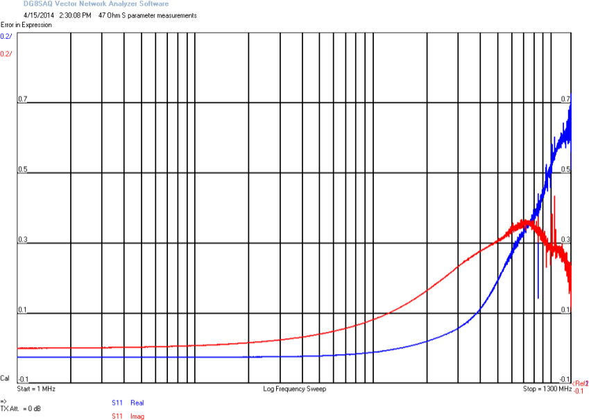 Figure 7 - DGSAQ Vector Network Analyser S parameter measurements for a 47 axial RF resistor.
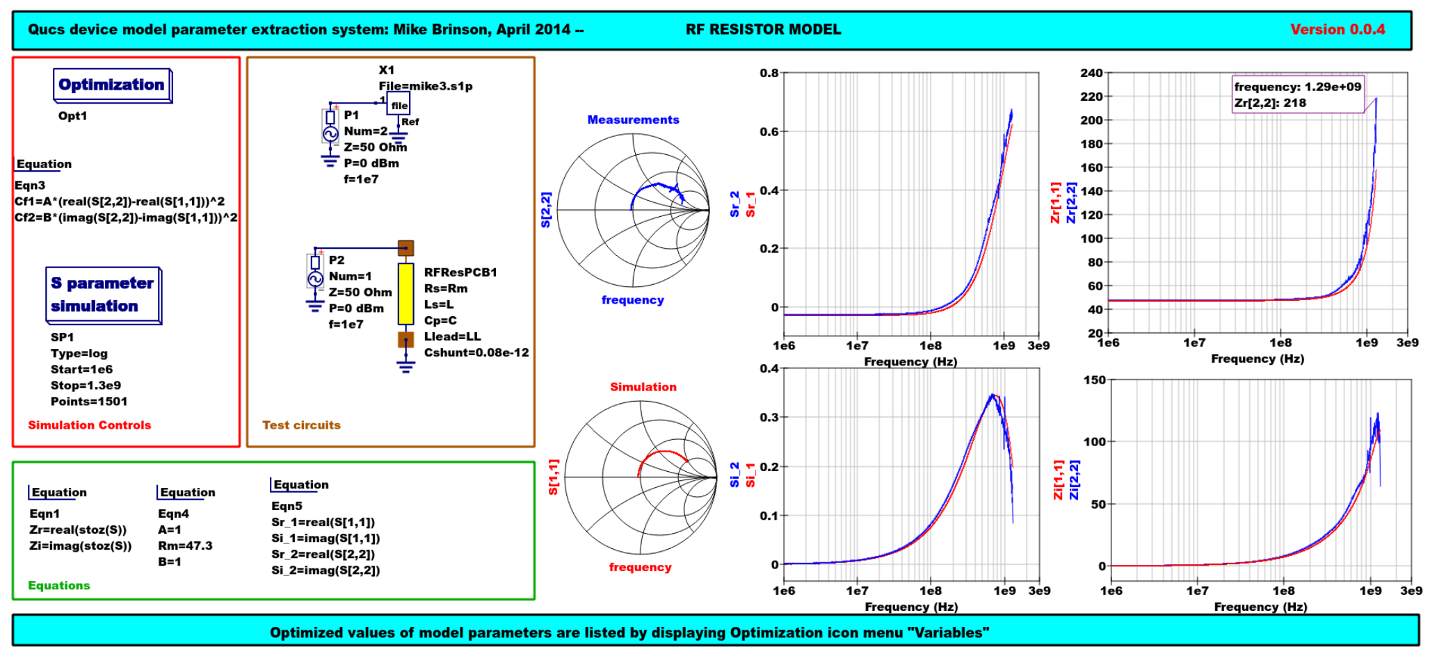 Figure 8 - Qucs device model parameter extraction system applied to a nominal 47 resistor represented by the subcircuit model illustrated in Figure 2 (c). Fixed model parameter values: Rs = Rm = 47.3 , CShunt = 0.08pF; Optimised values: Ls = L = 10.43nH, Llead = LL = 1.47nH, Cp = C = 0.69pF. To reduce simulation time the ASCO cost variance was set to 1e-3. The ASCO method was set to DE/best/1/exp.
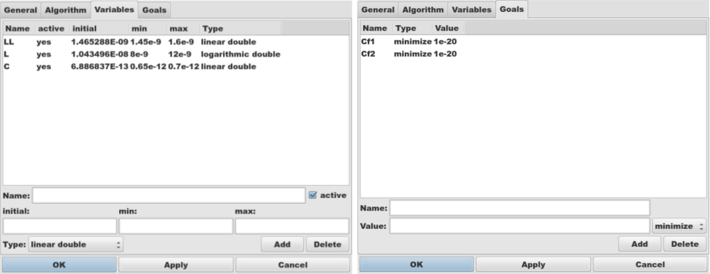 Figure 9 - Qucs Minimization Icon drop down menus: left ”Variables“ and right ”Goals``.
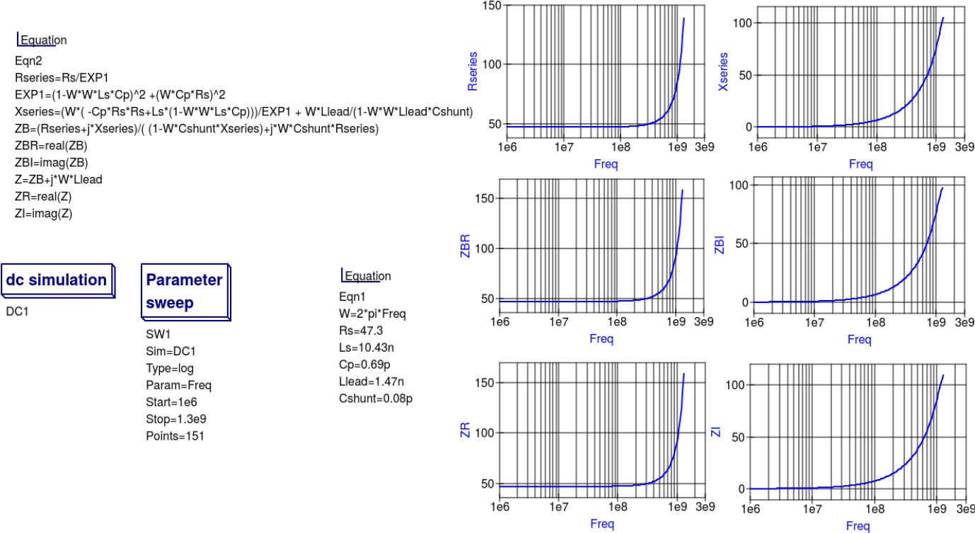 Figure 10 - Qucs simulation of nominal 47 resistor based on theoretical analysis.|
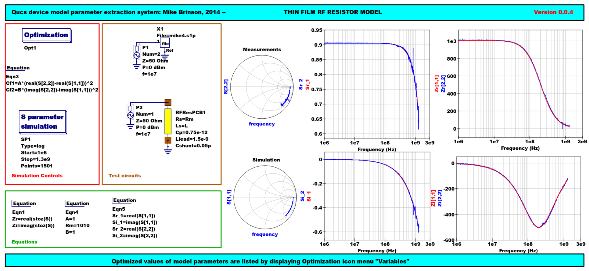 Figure 11 - Qucs device model parameter extraction system applied to a nominal 1000 resistor represented by the subcircuit model illustrated in Figure 2(c).
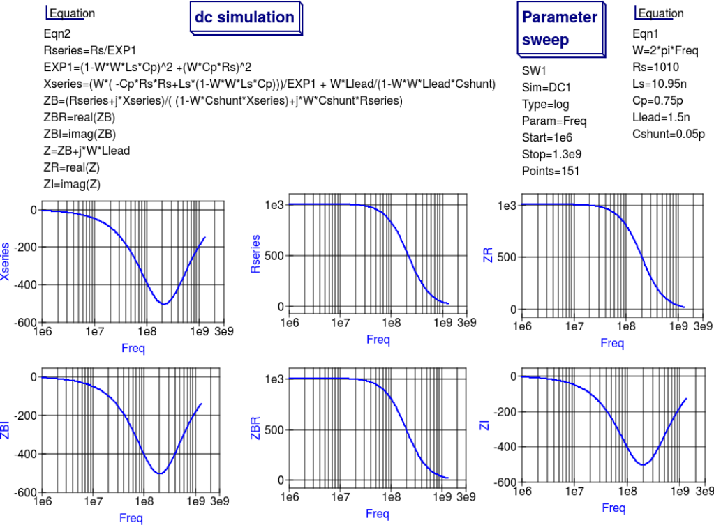 Figure 12 - Qucs simulation of nominal 1000 resistor based on theoretical analysis.
Extraction of RF resistor parameters from measured S data for a nominal 1000 axial resistor
At low resistance values the impedance of an RF resistor becomes inductive as the signal frequency is increased. This is due to the fact that the inductance Ls contribution dominates any reactance effects by Cp, Llead and Cshunt. However, as Rs is increased above a few hundred Ohm’s the reverse becomes true with reactive effects dominated by contributions from Cp. Figures 11 and 12 demonstrate the dominance of Cp reactive effects at low to mid-range frequencies.
One more example: extraction of RF resistor parameters fro measured S data for a nominal 100 SMD resistor
Figure 13 is included in this Qucs note purely for comparison purposes. SMD resistors are in general physically very small when compared to axial resistors. This results in lower values for the inductive and capacative parasitics which in turn ensures that the high frequency performance of SMD resistors is much improved.
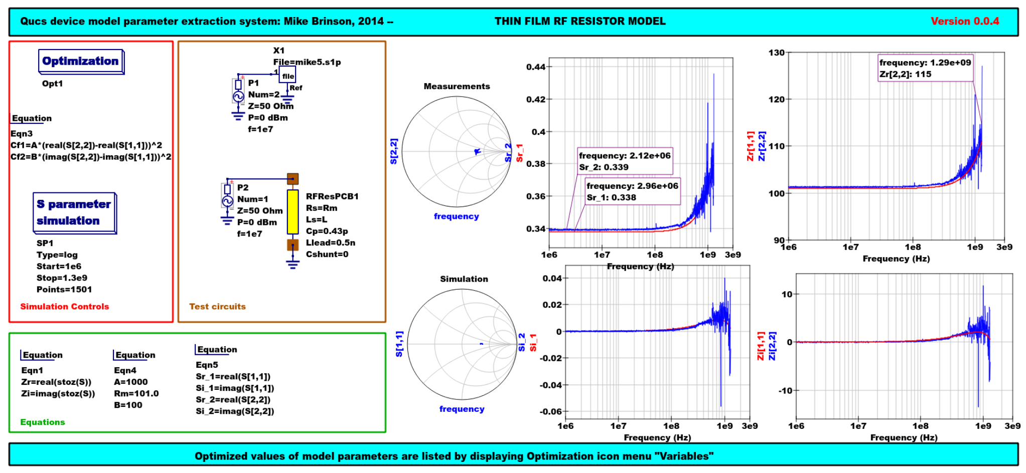 Figure 13 - Qucs device model parameter extraction system applied to a nominal 100 SMD resistor represented by the subcircuit model illustrated in Figure 2 (c).
A Verilog-A RF resistor model
Listed below is an example Verilog-A code model for the RF resistor model introduced in Figure 2 (c). Due to the limitations of the Verilog-A language subset provided by version 2.3.4 of the ”Analogue Device Model Synthesizer`` (ADMS) [4] inductors Ls and Llead are modelled by gyrators and capacitors with values identical to Ls or Llead.
//  Verilog-A module statement.
//
// RFresPCB.va  RF resistor (Thin film resistor, axial type, PCB mounting)
//
//   This is free software; you can redistribute it and/or modify
//   it under the terms of the GNU General Public License as published by
//   the Free Software Foundation; either version 2, or (at your option)
//   any later version.
//
//   Copyright (C), Mike Brinson, mbrin72043@yahoo.co.uk, April 2014.
//
`include "disciplines.vams"
`include "constants.vams"
//  Verilog-A module statement.
module RFresPCB(RT1, RT2);
inout RT1, RT2;              // Module external interface nodes.
electrical RT1, RT2;
electrical n1, n2, n3, nx, ny, nz;          // Internal nodes.
`define attr(txt) (*txt*)
parameter real Rs = 50         from [1e-20 : inf)
 `attr(info="RF resistance" unit="Ohm's");
parameter real Cp = 0.3e-12    from [0 : inf)
 `attr(info="Resistor shunt capacitance" unit="F");
parameter real Ls = 8.5e-9     from [1e-20 : inf)
 `attr(info="Series induuctance" unit="H");
parameter real Llead = 0.1e-9  from [1e-20 : inf)
 `attr(info="Parasitic lead induuctance" unit="H");
parameter real Cshunt = 1e-10  from [1e-20 : inf)
 `attr(info="Parasitic shunt capacitance" unit="F");
parameter real Tc1 = 0.0       from [-100  : 100]
 `attr(info="First order temperature coefficient" unit ="Ohm/Celsius");
parameter real Tc2 = 0.0       from [-100  : 100]
 `attr(info="Second order temperature coefficient" unit ="(Ohm/Celsius)^2");
parameter real Tnom  = 26.85   from [-273.15 : 300]
 `attr(info="Parameter extraction temperature" unit="Celsius");
parameter real Temp  = 26.85   from [-273.15 : 300]
 `attr(info="Simulation temperature" unit="Celsius");
branch (RT1, n1)  bRT1n1;    // Branch statements
branch (n1, n2)   bn1n2;
branch (n1, n3)   bn1n3;
branch (n2, n3)   bn2n3;
branch (n3, RT2)  bn3RT2;
real Rst, FourKT, n, Tdiff, Rn;
analog begin  // Start of analog code
@(initial_model)
 begin
   Tdiff = Temp-Tnom;   FourKT =4.0*`P_K*Temp;
   Rst = Rs*(1.0+Tc1*Tdiff+Tc2*Tdiff*Tdiff);  Rn     = FourKT/Rst;
 end
 I(n1)     <+ ddt(Cshunt*V(n1));   I(bn1n2)  <+ V(bn1n2)/Rst;
 I(bn1n3)  <+ ddt(Cp*V(bn1n3));    I(n3)     <+ ddt(Cshunt*V(n3));
 I(bRT1n1)  <+ -V(nx); I(nx)      <+ V(bRT1n1);   // Llead
 I(nx)      <+ ddt(Llead*V(nx));
 I(bn2n3)   <+ -V(ny);  I(ny)      <+ V(bn2n3);  // Ls
 I(ny)      <+ ddt(Ls*V(ny));
 I(bn3RT2)  <+ -V(nz);  I(nz)      <+ V(bn3RT2);   // Llead
 I(nz)      <+ ddt(Llead*V(nz));
 I(bn1n2)    <+ white_noise(Rn, "thermal");  // Noise contribution
end  // End of analog code
endmodule
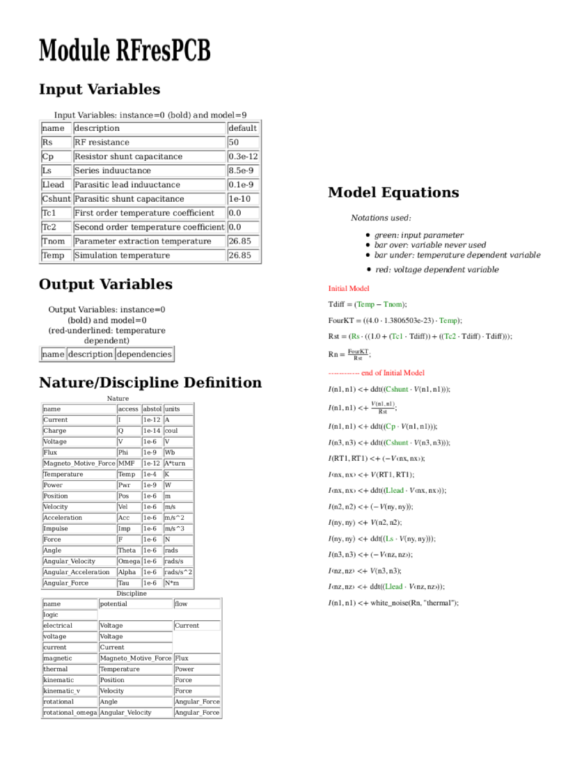 Figure 14 - Details of the proposed RF resistor model: equations, variables and other data.
Extraction of Verilog-A RF resistor model parameters from measured S data for a 100 axial resistor
This example demonstrates the use of ASCO for extracting Verilog-A model parameters from measured S parameter data. ASCO optimization yields a figure of 4nH for L in the model shown in Figure 2 (c). Other model parameter values are given with the test circuit, see Figure 15.
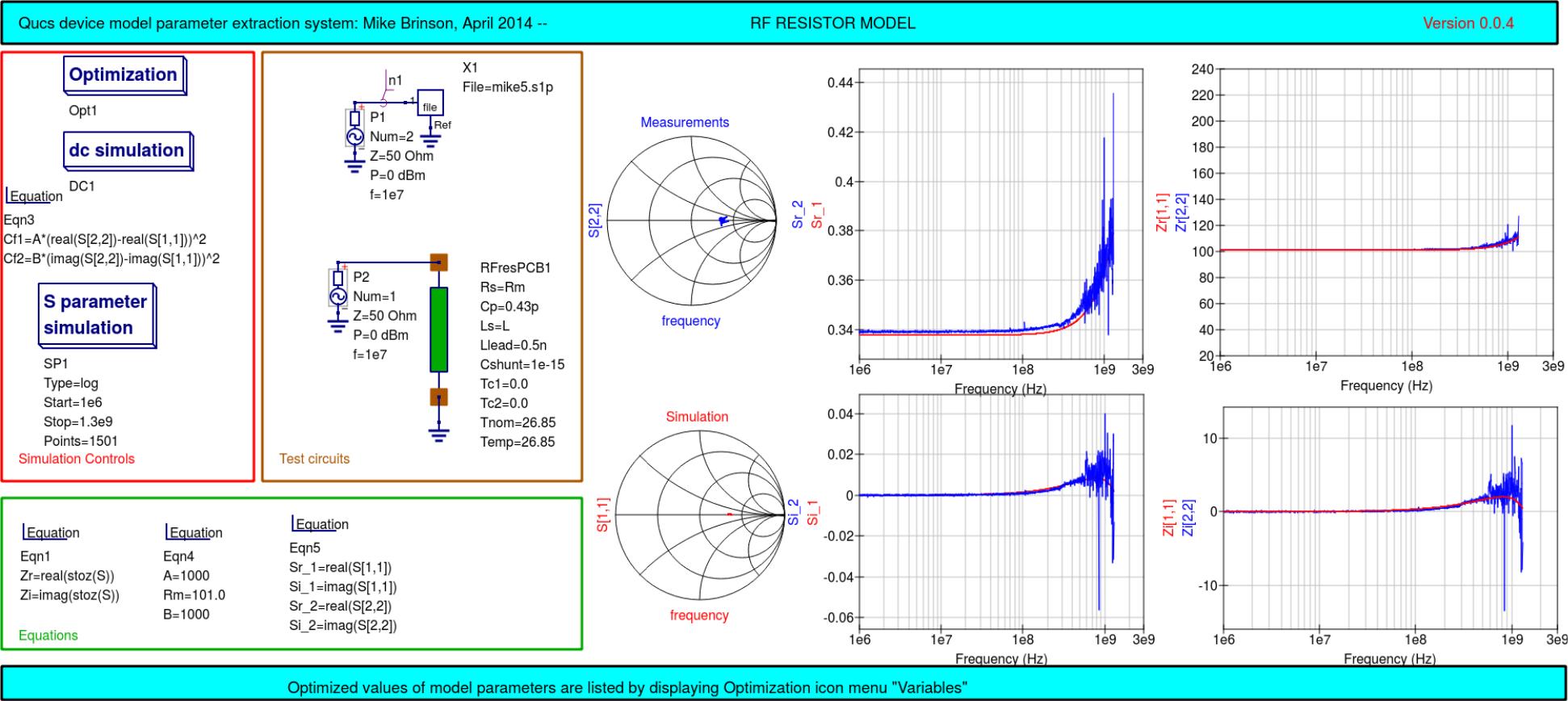 Figure 15 - Verilog-A models parameter data extraction for a 100 axial thin film resistor. Fixed model parameter values: Rs = Rm =101 , CShunt = 1e-15 F, Llead = LL = 0.5nH, Cp = C = 0.43pF; Optimised values: Ls = L = 3.99nH. To reduce simulation time the ASCO cost variance was set to 1e-3. The ASCO method was set to DE/best/1/exp.
End Notes
This brief Qucs note outlines the fundamental properties of subicircuit and verilog-A compact component models for RF resistors. The use of optimization for the extraction of subcircuit and Verilog-A compact model parameters from measured S parameters is also demonstrated. The presented techniques form part of the simulation and device modelling capabilities available with the latest Qucs release [5].
| [1] | DG8SAQ VNWA 3 & 3E- Vector Network Analysers, SDR Kits Limited, Grangeside Business Centre, 129 Devizes Road, Trowbridge, Wilts, BA14-7sZ, United Kingdom, 2014. |
| [2] | See DG8SAQ VNWA 3 & 3E- Vector Network Analysers- Getting Started Manual for Windows 7, Vista and Windows XP. |
| [3] | (http://www.vhdl.org/ibis/connector/touchstone_spec11.pdf). |
| [4] | (http://sourceforge.net/projects/mot-adms/). |
| [5] | Qucs release 0.0.18, or greater. |